dc step up buck converter. Voltage converter dc dc circuit and operation. Pulse Width Modulation - PWM
Company STMicroelectronics manufactures high-quality non-isolated DC/DC converter ICs that require few external components.
The constant development of ICs for DC/DC converters is characterized by the following factors:
- an increase in the operating conversion frequencies (the maximum conversion frequency for STMicroelectronics microcircuits is 1.7 MHz), which makes it possible to drastically reduce the size of external components and minimize the area of the printed circuit board;
- reduction in the size of microcircuit packages due to high conversion frequencies (the DFN6D package has dimensions of only 3x3mm);
- promotion specific gravity output current (the DFN6D package provides output current up to 2.0A; the DFN8 and PowerSO-8 packages can operate at currents up to 3.0A);
- an increase in efficiency and a decrease in power consumption in the off state, which is especially important for self-powered devices.
STM divides its ICs for non-isolated DC/DC converters into two groups. The first group has an operating frequency of up to 1 MHz (the parameters are summarized in Table 1), the second group has a conversion frequency of 1.5 and 1.7 MHz (see Table 2 for the parameters). The second group also includes microcircuits of the series ST1S10 with a nominal conversion frequency of 0.9 MHz (the maximum conversion frequency for these chips can reach 1.2 MHz). Microcircuits of the ST1S10 series can work with synchronization from an external generator in the frequency range from 400 kHz to 1.2 MHz.
Table 1. Chips STMicroelectronics for DC / DC-converters with a conversion frequency up to 1 MHz
| Name | Topology | Vin., V | Vout., V | Iout., A | Frequency conversion, MHz |
entrance blackouts |
Frame |
|---|---|---|---|---|---|---|---|
| L296 | step down | 9…46 | 5,1…40 | 4 | up to 200 | There is | MULTIWATT-15 |
| L4960 | step down | 9…46 | 5,1…40 | 2,5 | up to 200 | Not | HEPTAWATT-7 |
| L4962 | step down | 9…46 | 5,1…40 | 1,5 | up to 200 | There is | HEPTAWATT-8, DIP-16 |
| L4963 | step down | 9…46 | 5,1…40 | 1,5 | 42…83 | Not | DIP-18, SO-20 |
| L4970A | step down | 12…50 | 5,1…50 | 10 | up to 500 | Not | MULTIWATT-15 |
| L4971 | step down | 8…55 | 3,3…50 | 1,5 | up to 300 | There is | DIP-8, SO-16W |
| L4972A | step down | 12…50 | 5,1…40 | 2 | up to 200 | Not | DIP-20, SO-20 |
| L4973D3.3 | step down | 8…55 | 0,5…50 | 3,5 | up to 300 | There is | DIP-8, SO-16W |
| L4973D5.1 | step down | 8…55 | 5,1…50 | 3,5 | up to 300 | There is | DIP-8, SO-16W |
| L4974A | step down | 12…50 | 5,1…40 | 3,5 | up to 200 | Not | MULTIWATT-15 |
| L4975A | step down | 12…50 | 5,1…40 | 5 | up to 500 | Not | MULTIWATT-15 |
| L4976 | step down | 8…55 | 0,5…50 | 1 | up to 300 | There is | DIP-8, SO-16W |
| L4977A | step down | 12…50 | 5,1…40 | 7 | up to 500 | Not | MULTIWATT-15 |
| L4978 | step down | 8…55 | 3,3…50 | 2 | up to 300 | There is | DIP-8, SO-16W |
| L5970AD | step down | 4,4…36 | 0,5…35 | 1 | 500 | There is | SO-8 |
| L5970D | step down | 4,4…36 | 0,5…35 | 1 | 250 | There is | SO-8 |
| L5972D | step down | 4,4…36 | 1,23…35 | 1,5 | 250 | Not | SO-8 |
| L5973AD | step down | 4,4…36 | 0,5…35 | 1,5 | 500 | There is | HSOP-8 |
| L5973D | step down | 4,4…36 | 0,5…35 | 2 | 250 | There is | HSOP-8 |
| L5987A | step down | 2,9…18 | 0.6…Vin. | 3 | 250…1000 | There is | HSOP-8 |
| L6902D | step down | 8…36 | 0,5…34 | 1 | 250 | Not | SO-8 |
| L6920D | step-up | 0,6…5,5 | 2…5,2 | 1 | up to 1000 | There is | TSSOP-8 |
| L6920DB | step-up | 0,6…5,5 | 1,8…5,2 | 0,8 | up to 1000 | There is | miniSO-8 |
Table 2. ICs for DC/DC buck converters from 0.9 to 1.7 MHz
| Series | Name | Iout., A | Vin., V | Vout., V | Frequency conversion, MHz |
entrance blackouts |
Frame |
|---|---|---|---|---|---|---|---|
| ST1S03 | ST1S03PUR | 1,5 | 3…16 | 0,8…12 | 1,5 | Not | DFN6D (3x3 mm) |
| ST1S03A | ST1S03AIPUR | 3…5.5 | 0,8…5.5 | 1,5 | There is | DFN6D (3x3 mm) | |
| ST1S03APUR | 1,5 | Not | |||||
| ST1S06 | ST1S06PUR | 2,7…6 | 0,8…5.5 | 1,5 | There is | DFN6D (3x3 mm) | |
| ST1S06A | ST1S06APUR | 1,5 | Not | ||||
| ST1S06xx12 | ST1S06PU12R | 2,7…6 | 1,2 | 1,5 | There is | DFN6D (3x3mm) | |
| ST1S06xx33 | ST1S06PU33R | 3,3 | 1,5 | There is | |||
| ST1S09 | ST1S09IPUR | 2,0 | 2,7…5,5 | 0,8…5 | 1,5 | There is | DFN6D (3x3 mm) |
| ST1S09PUR | 1,5 | Not | |||||
| ST1S10 | ST1S10PHR | 3,0 | 2,5…18 | 0.8…0.85Vin. | 0,9 (0,4…1,2)* | There is | PowerSO-8 |
| ST1S10PUR | DFN8 (4x4mm) | ||||||
| ST1S12xx | ST1S12GR | 0,7 | 2,5…5,5 | 1,2…5 | 1,7 | There is | TSOT23-5L |
| ST1S12xx12 | ST1S12G12R | 1,2 | |||||
| ST1S12xx18 | ST1S12G18R | 1,8 | |||||
| * - in parentheses is the conversion frequency range when synchronizing from an external generator. | |||||||
The main part of microcircuits for DC/DC converters from Table 1 has a conversion frequency of up to 300 kHz. At such frequencies, the choice of inductances at the DC / DC output is facilitated, since for the operating frequencies of the microcircuits from Table 2 (1.5 and 1.7 MHz), it is necessary to pay attention to the frequency characteristics of the inductances Special attention. Figures 1 and 2 show the manufacturer's recommended circuits for switching microcircuits as examples. L5973D(output current up to 2.0 A at a conversion frequency of 250 kHz) and ST1S06(output current up to 1.5 A at a conversion frequency of 1.5 MHz).
Rice. one.

Rice. 2.
Figures 1 and 2 show that ICs with relatively low conversion frequencies by today's standards require a larger number of external electronic components that are larger than the components of converters operating at frequencies above 1 MHz. The DC/DC ICs in Table 2 provide much smaller board sizes, but more care must be taken in wiring to reduce radiated EMI.
Some microcircuits allow you to control the on and off of the converters due to the presence of the INHIBIT input. An example of the inclusion of such microcircuits is shown in Fig. 3. ST1S09(without INHIBIT input) and ST1S09I(with INHIBIT input). The bottom of this figure shows the recommended values of resistors R1 and R2 for generating output voltages of 1.2 and 3.3 V.

Rice. 3.
If there is a high voltage level (more than 1.3 V) at the VINH control input, the ST1S09I microcircuit is in the active state; if the voltage at this input is less than 1.4 V, the DC/DC converter turns off (self-consumption is less than 1 µA). A variant of the microcircuit without a control input on pin 6 instead of the VINH input has the output "PG = Power Good" (power is normal). The formation of the "Power Good" signal is illustrated in fig. 4. When the FB input (FeedBack or feedback input) reaches 0.92xVFB, the comparator switches and the PG output goes high to indicate that the output voltage is within acceptable limits.

Rice. 4.
Conversion efficiency
on the example of ST1S09 and ST1S09I microcircuits
The efficiency of a DC/DC buck converter is highly dependent on the parameters of the insulated gate transistors (MOSFETs) integrated into the microcircuits, which act as a key. One of the problems with high-frequency converters is related to the transistor gate charge current when controlled by a PWM controller. Losses in this case practically do not depend on the current in the load. The second problem that reduces efficiency is the power dissipated in the transistor during switching from one state to another (during these periods of time, the transistor operates in a linear mode). You can reduce losses by providing steeper switching fronts, but this increases electromagnetic noise and interference in the power circuits. Another reason for reducing the efficiency of the converter is the presence of active resistance "drain - source" (Rdson). In a properly designed circuit, the efficiency reaches its maximum value when the static (ohmic) and dynamic losses are equal. It should be noted that the output rectifier diode also contributes its share of dynamic and static losses. An incorrectly chosen inductance at the output of a DC / DC converter can further significantly reduce the conversion efficiency, which makes one remember about its high-frequency properties. In the worst case, at high conversion frequencies, the output choke may lose its inductive properties, and the converter simply will not work.
STMicroelectronics has been producing high power FETs and diodes with very high dynamic and static characteristics for many years. Possession of well-established MOSFET technology allows the company to integrate its field-effect transistors into microcircuits for DC/DC converters and achieve high conversion efficiency values.
On fig. 5 (a, b, c) as an example, typical dependences of the conversion efficiency on some parameters under different operating conditions are shown. Graphs of the dependence of efficiency on the value of the output current reach maximum values of about 95% at a current of 0.5 A. Further, the decline in these characteristics is rather gentle, which characterizes only a slight increase in losses with an increase in the output current to a maximum value.

Rice. 5a.
On fig. Figure 5b shows the dependence of the efficiency on the output voltage level of DC/DC converters based on ST1S09 and ST1S09I microcircuits. As the output voltage increases, the efficiency increases. This is due to the fact that the voltage drop across the transistors of the output stage is practically independent of the output voltage at a constant output current, therefore, as the output voltage increases, the percentage of insertion loss will decrease.

Rice. 5 B.
On fig. 5c shows the dependence of the efficiency on the value of the inductance at the output. In the range from 2 to 10 μH, the conversion efficiency practically does not change, which allows you to choose the value of the inductance from a wide range of ratings. Of course, one should strive for the highest possible level of inductance to provide the best voltage filtering of the output current ripple. It is clear that as the output current increases, the efficiency decreases. This is due to the increase in losses in the output stages of DC/DC converters.

Rice. 5th century
Comparison with chips from other manufacturers
Tables 3, 4 and 5 show parameters close in functional value chips from other manufacturers.
Table 3 shows that FAN2013MPX is a complete analogue for a microcircuit ST1S09IPUR, but STMicroelectronics additionally has a chip in this series ST1S09PUR with the presence of the output "Power Good", which expands the choice of the developer.
Table 3 Close replacements for ICs for DC/DC converters from other manufacturers
| Manufacturer | Name | Iout max., A | Frequency conversion, MHz |
power good | Compatibility according to the findings |
Frame |
|---|---|---|---|---|---|---|
| STMicroelectronics | ST1S09PUR | 2 | 1,5 | There is | There is | DFN3x3-6 |
| ST1S09IPUR | Not | There is | ||||
| Fairchild Semiconductor | FAN2013MPX | 2 | 1,3 | Not | There is | DFN3x3-6 |
Table 4 lists functional replacements (no pin compatibility) from other manufacturers for ICs ST1S10. The main advantage of ST1S10 microcircuits is the presence of synchronous rectification in the output stages, which provides more high efficiency transformations. In addition, the DFN8 package (4x4 mm) has smaller dimensions compared to the packages of functionally similar microcircuits from other manufacturers. The internal compensation circuit reduces the number of external chip piping components.
Table 4 Close replacements for ST1S10PxR ICs for DC/DC buck converters from other manufacturers
| Manufacturer | Name | Iout max., A | Synchronous rectification | Compensation | Soft start | Compatibility according to the findings |
Frame |
|---|---|---|---|---|---|---|---|
| STMicroelectronics | ST1S10PHR | 3 | There is | Internal | Interior | - | PowerSO-8 |
| ST1S10PUR | DFN8 (4x4mm) | ||||||
| Monolithic Power Systems | MP2307/MP1583 | 3 | Yes/No | External | External | Not | SO8-EP |
| Alpha & Omega Semiconductor | AOZ1013 | 3 | Not | External | Interior | Not | SO8 |
| Semtech | SC4521 | 3 | Not | External | External | Not | SO8-EP |
| AnaChip | AP1510 | 3 | Not | Internal | Interior | Not | SO8 |
Table 5 shows possible replacements for ICs ST1S12. The main advantage of the ST1S12 microcircuits is the higher value of the maximum allowable output current: up to 700 mA. The MP2104 chip from MPS is pin-compatible with the ST1S12 chip. The LM3674 and LM3671 can only be considered as a close functional replacement for the ST1S112 due to the lack of pin compatibility.
Table 5 Close replacements for ST1S12 ICs for DC/DC buck converters from other manufacturers
| Manufacturer | Name | Iout (max.), mA |
Frequency conversion, MHz |
Vin (max.), V | entrance blackouts |
Compatibility according to the findings |
Frame |
|---|---|---|---|---|---|---|---|
| STMicroelectronics | ST1S12 | 700 | 1,7 | 5,5 | there is | - | TSOT23-5L |
| Monolithic Power Systems | MP2104 | 600 | 1,7 | 6 | there is | there is | TSOT23-5L |
| National Semiconductor | LM3674 | 600 | 2 | 5,5 | there is | No | SOT23-5L |
| LM3671 | 600 | 2 | 5,5 | there is | No | SOT23-5L |
Chip selection for
DC/DC converters on site
To quickly search for electronic components by known parameters, it is most convenient to use the site . For parametric search on this site, it is highly recommended to install and use a free site viewer (browser)" Google Chrome". Working in this browser speeds up the search several times. Chips for DC / DC converters from STMicroelectronics can be found on the website along the following path: "Power Management" ® "IC for DC / DC" ® "Regulators (+ key)". Next, you can select the brand "ST" and activate the "Stock" filter to select only those components that are in stock. The result of these actions is shown in Fig. 6. You can make a more specific selection on the required parameters by applying other filters.
Conclusion
Especially important right choice microcircuits for DC/DC converters in devices with autonomous power supplies. In some cases, choosing the right power plan can be a difficult task, but by taking the time to design and select a device's power plan, you can gain some edge over the competition with a smaller, lower cost, higher power conversion efficiency solution. STMicroelectronics ICs for DC/DC converters make it easy to choose and realize their advantages when creating competitive power schemes.
Obtaining technical information, ordering samples, delivery - e-mail:
This DC-DC Converter voltage from 5-13V input, up to 12V DC output 1.5A. Converter takes less voltage and gives higher output to use where there is voltage less than the required 12 volts. Often it is used to increase the voltage of existing batteries. This is essentially an integrated DC-DC converter. For example: there is a 3.7V Li-Ion battery, and its voltage can be changed using this circuit to provide the required 12V at 1.5A.
The converter is easy to build yourself. The main component is the MC34063 IC, which consists of a voltage reference (temperature compensated), a comparator, an oscillator with an active peak current limiting circuit, a gate (“AND” element), a flip-flop and a high-power output switch with a driver, and only a few additional electronic components are required. in a harness so that it is ready. This series of microcircuits has been specially designed to be included in various converters.

Advantages of the MC34063A chip
- Work from 3 to 40V input
- Low standby current
- current limit
- Output current up to 1.5 A
- Output voltage adjustable
- Operation in the frequency range up to 100 kHz
- Accuracy 2%

Description of radio elements
- R- All resistors are 0.25W.
- T- TIP31-NPN power transistor. All output current passes through it.
- L1- 100 µH ferrite coils. If you have to do it yourself, you need to purchase toroidal ferrite rings with an outer diameter of 20 mm and an inner diameter of 10 mm, also 10 mm high and a wire 1 - 1.5 mm thick by 0.5 meters, and make 5 turns at equal distances. The dimensions of the ferrite ring are not too critical. A few (1-3mm) difference is acceptable.
- D- Schottky diode must be used
- TR- a multi-turn variable resistor, which is used here to fine-tune the 12 V output voltage.
- C- C1 and C3 are polarized capacitors, so pay attention to this when placing them on the PCB.


Assembly parts list
- Resistors: R1 = 0.22 ohm x1, R2 = 180 ohm x1, R3 = 1.5K x1, R4 = 12K x1
- Regulator: TR1 = 1 kΩ, multi-turn
- Transistor: T1 = TIP31A or TIP31C
- Choke: L1 = 100 uH on ferrite ring
- Diode: D1 - Schottky 1N5821 (21V - 3A), 1N5822 (28V - 3A) or MBR340 (40V - 3A)
- Capacitors: C1 = 100uF / 25V, C2 = 0.001uF, C3 = 2200uF / 25V
- Chip: MC34063
- PCB 55 x 40 mm

Note that it is necessary to set a small aluminum radiator to transistor T1 - TIP31, otherwise this transistor may be damaged due to increased heating, especially at high load currents. Datasheet and PCB drawing
As you know, white and blue LEDs need at least 3V to light up, unlike red LEDs which can glow from 1.2 to 1.5 volts depending on the type.
In order for the white LED to start glowing from one 1.5 volt battery, it is necessary to build electronic circuit entitled . These devices are typically used to produce a higher voltage output compared to a direct current (DC) input.
In circuits with alternating current, this function. To get a higher output voltage, it is enough that the ratio of the number of turns of the secondary winding to the number of primary windings is greater than 1 (transformation ratio > 1).
Description of the operation of the converter for the LED
Returning to our DC/DC converter, there are many various options implementations of DC-DC conversion, many of which are quite complex. In our case, the goal is to create a simple and efficient converter circuit for stepping up the voltage from 1.5V to 3.5V. Below is a diagram of a similar DC-DC converter for LEDs.

To wind the inductor, ferrite is required, the shape and size of which can be any, but it is better to use a “ring” (or torus) core 1 ... 1.5 cm in diameter. This is usually used as a filter on power supply wires (black block next to the connector), and can also be found in switching power supplies, VCRs, scanners, etc. The winding is made with PEV-2 wire with a diameter of 0.4 mm and contains 30 turns.

The electronic circuit is very simple: it consists of a coil, two transistors, one capacitor and two resistors. The set is not impressive, but it does its job. The current consumption is 25 mA, which is equivalent to approximately 50 hours of continuous operation of an AA battery. The circuit works quite well, providing an average level of illumination of the LED.
The LM2596 steps down the input (up to 40V) voltage - the output is regulated, the current is 3A. Ideal for LEDs in the car. Very cheap modules - about 40 rubles in China.
Texas Instruments produces high-quality, reliable, affordable and cheap, easy-to-use DC-DC controllers LM2596. Chinese factories produce ultra-cheap stepdown converters based on it: the price of a module for an LM2596 is about 35 rubles (including delivery). I advise you to buy immediately a batch of 10 pieces - there will always be a use for them, while the price will drop to 32 rubles, and less than 30 rubles when ordering 50 pieces. Read more about the calculation of the strapping of the microcircuit, adjusting the current and voltage, its application and some of the disadvantages of the converter.
A typical method of use is a stabilized voltage source. Based on this stabilizer, it is easy to make impulse block power supply, I use it as a simple and reliable laboratory block short circuit power supply. They are attractive due to the consistency of quality (it seems that they are all made in the same factory - and it is difficult to make mistakes in five details), and full compliance with the datasheet and the declared characteristics.
Another area of application is a switching current stabilizer for food powerful LEDs . The module on this chip will allow you to connect a 10-watt automotive LED matrix, additionally providing short circuit protection.
I highly recommend buying a dozen of them - they will definitely come in handy. They are unique in their own way - the input voltage is up to 40 volts, and only 5 external components are required. This is convenient - you can raise the voltage on the smart home power bus to 36 volts by reducing the cross section of the cables. We install such a module at consumption points and set it to the required 12, 9, 5 volts, or as much as you need.
Let's consider them in more detail.
Chip characteristics:
- Input voltage - from 2.4 to 40 volts (up to 60 volts in the HV version)
- Output voltage - fixed or adjustable (from 1.2 to 37 volts)
- Output current - up to 3 amperes (with good cooling - up to 4.5A)
- Conversion frequency - 150kHz
- Enclosure - TO220-5 (hole mount) or D2PAK-5 (surface mount)
- Efficiency - 70-75% at low voltages, up to 95% at high voltages
- Stabilized voltage source
- Converter circuit
- datasheet
- USB charger based on LM2596
- current stabilizer
- Application in homemade devices
- Adjustment of output current and voltage
- Improved analogues of LM2596
History - Linear Stabilizers
To begin with, I will explain why standard linear voltage converters like LM78XX (for example 7805) or LM317 are bad. Here is his simplified diagram.
The main element of such a converter is a powerful bipolar transistor, included in its "original" meaning - as a controlled resistor. This transistor is part of a Darlington pair (to increase the current transfer ratio and reduce the power required to operate the circuit). Base current is set operational amplifier, which amplifies the difference between the output voltage and the one set using the ION (reference voltage source), i.e. it is included according to the classical error amplifier circuit.
Thus, the converter simply includes a resistor in series with the load, and controls its resistance so that, for example, exactly 5 volts is extinguished at the load. It is easy to calculate that when the voltage drops from 12 volts to 5 (a very common case of using the 7805 microcircuit), the input 12 volts are distributed between the stabilizer and the load in the ratio “7 volts at the stabilizer + 5 volts at the load”. At a half-amp current, 2.5 watts are released on the load, and at 7805 - as much as 3.5 watts.
It turns out that the "extra" 7 volts are simply extinguished on the stabilizer, turning into heat. Firstly, because of this, there are problems with cooling, and secondly, it takes a lot of energy from the power supply. When powered from a wall outlet, this is not very scary (although it still harms the environment), but when using battery or rechargeable batteries, one cannot help but remember this.
Another problem is that it is generally impossible to make a boost converter with this method. Often such a need arises, and attempts to solve this issue twenty or thirty years ago are striking - how complicated was the synthesis and calculation of such schemes. One of the simplest circuits of this kind is a 5V->15V push-pull converter.
It must be admitted that it provides galvanic isolation, but it uses the transformer inefficiently - only half of the primary winding is involved at any time.
Let's forget it like a bad dream and move on to modern circuitry.
Voltage source
Scheme
The microcircuit is convenient to use as a step-down converter: a powerful bipolar switch is inside, it remains to add the rest of the regulator components - a fast diode, an inductance and an output capacitor, it is also possible to put an input capacitor - only 5 parts.
The LM2596ADJ version will also require an output voltage setting circuit, these are two resistors or one variable resistor.
Step-down voltage converter circuit based on LM2596:
The whole scheme together:
Here you can download datasheet for LM2596.
How it works: A PWM controlled high power switch inside the device sends voltage pulses to an inductor. At point A x% of the time the full voltage is present and (1-x)% of the time the voltage is zero. The LC filter smooths out these fluctuations by extracting a DC component equal to x * supply voltage. The diode closes the circuit when the transistor is off.
Detailed job description
An inductor opposes a change in current through it. When voltage appears at point A, the inductor creates a large negative self-induction voltage, and the voltage across the load becomes equal to the difference between the supply voltage and the self-induction voltage. The inductance current and the load voltage gradually increase.
After the voltage disappears at point A, the inductor seeks to maintain the same current flowing from the load and the capacitor, and closes it through the diode to the ground - it gradually drops. Thus, the voltage at the load is always less than the input voltage and depends on the duty cycle of the pulses.
Output voltage
The module is available in four versions: with a voltage of 3.3V (index -3.3), 5V (index -5.0), 12V (index -12) and an adjustable version LM2596ADJ. It makes sense to use the custom version everywhere, since it is in large quantities in the warehouses of electronic companies and you are unlikely to encounter a shortage of it - and it requires an additional two penny resistors. And of course, the 5 volt version is also popular.
Quantity in stock is in the last column.
You can set the output voltage in the form of a DIP switch, good example shown here, or as a rotary switch. In both cases, you will need a battery of precise resistors - but you can adjust the voltage without a voltmeter.
Frame
There are two housing options: TO-263 planar mount housing (model LM2596S) and through-hole mount TO-220 housing (model LM2596T). I prefer the planar version of the LM2596S because the heatsink is the board itself and there is no need to purchase an additional external heatsink. In addition, its mechanical resistance is much higher, unlike TO-220, which must be screwed to something, even to the board - but then it is easier to install the planar version. I recommend using the LM2596T-ADJ chip in power supplies, because it is easier to remove from its case a large number of heat.
Smoothing input voltage ripple
Can be used as an effective "intelligent" stabilizer after rectifying the current. Since the IC monitors the output voltage directly, fluctuations in the input voltage will cause the IC's conversion ratio to change inversely, and the output voltage will remain normal.
It follows from this that when using the LM2596 as a step-down converter after the transformer and rectifier, the input capacitor (i.e. the one that stands immediately after the diode bridge) can have a small capacitance (about 50-100uF).
output capacitor
Due to the high conversion frequency, the output capacitor also does not have to have a large capacitance. Even a powerful consumer will not have time to significantly plant this capacitor in one cycle. Let's carry out the calculation: take a capacitor of 100uF, 5V output voltage and a load that consumes 3 amperes. The total charge of the capacitor q \u003d C * U \u003d 100e-6 uF * 5 V \u003d 500e-6 uC.
In one conversion cycle, the load will take dq = I * t = 3 A * 6.7 μs = 20 μC from the capacitor (this is only 4% of the total charge of the capacitor), and a new cycle will immediately begin, and the converter will put a new portion of energy into the capacitor.
Most importantly, do not use tantalum capacitors as input and output capacitors. They write right in the datasheets - “do not use in power circuits”, because they do not tolerate even short-term voltage surges very well, and do not like high impulse currents. Use regular aluminum electrolytic capacitors.
Efficiency, efficiency and heat loss
The efficiency is not so high, since a bipolar transistor is used as a powerful key - and it has a non-zero voltage drop, of the order of 1.2V. Hence the drop in efficiency at low voltages.
As you can see, the maximum efficiency is achieved with a difference between the input and output voltages of the order of 12 volts. That is, if you need to reduce the voltage by 12 volts, the minimum amount of energy will go into heat.
What is converter efficiency? This is a value that characterizes the current losses - for the release of heat on a fully open powerful key according to the Joule-Lenz law and for similar losses during transients - when the key is open, say, only half. The effects of both mechanisms can be comparable in magnitude, so we should not forget about both ways of loss. A small amount of power is also used to power the “brains” of the converter itself.
In the ideal case, when the voltage is converted from U1 to U2 and the output current is I2, the output power is P2 = U2*I2, the input power is equal to it (ideal case). This means that the input current will be I1 = U2/U1*I2.
In our case, the conversion has an efficiency below unity, so part of the energy will remain inside the device. For example, with efficiency η, the output power will be P_out = η*P_in, and losses P_loss = P_in-P_out = P_in*(1-η) = P_out*(1-η)/η. Of course, the converter will be forced to increase the input current in order to maintain the specified output current and voltage.
We can assume that when converting 12V -> 5V and an output current of 1A, the losses in the microcircuit will be 1.3 watts, and the input current will be 0.52A. In any case, this is better than any linear converter, which will give a minimum of 7 watts of losses, and will consume 1 ampere from the input network (including for this useless business) - twice as much.
By the way, the LM2577 chip has a three times lower frequency of operation, and its efficiency is slightly higher, since there are less losses in transients. However, it needs three times the inductor and output capacitor ratings, which is extra money and board size.
Increasing the output current
Despite the already rather large output current of the microcircuit, sometimes even more current is required. How to get out of this situation?
- You can parallel multiple converters. Of course, they must be set exactly to the same output voltage. In this case, you cannot do with simple SMD resistors in the Feedback voltage setting circuit, you must either use resistors with an accuracy of 1%, or manually set the voltage with a variable resistor.
USB charger on LM2596
You can make a very convenient camping USB charger. To do this, you need to set the regulator to a voltage of 5V, provide it with a USB port and provide power to the charger. I'm using a radio model lithium polymer battery purchased from China that delivers 5 amp-hours at 11.1 volts. That's a lot - enough to 8 times charge a regular smartphone (not taking into account efficiency). Taking into account the efficiency, it will turn out at least 6 times.
Don't forget to short the D+ and D- pins of the USB socket to tell the phone that it is connected to the charger and that the transmitted current is unlimited. Without this event, the phone will think that it is connected to a computer and will be charged with a current of 500mA - for a very long time. Moreover, such a current may not even compensate for the current consumption of the phone, and the battery will not charge at all.
You can also provide a separate 12V input from a car battery with a cigarette lighter socket - and switch sources with some kind of switch. I advise you to install an LED that will signal that the device is on, so as not to forget to turn off the battery after a full charge - otherwise the losses in the converter will completely drain the backup battery in a few days.
Such a battery is not very suitable, because it is designed for high currents - you can try to find a less high-current battery, and it will be smaller and lighter.
current stabilizer
Output current adjustment
Only available in configurable output voltage version (LM2596ADJ). By the way, the Chinese also make such a version of the board, with voltage and current adjustment and all kinds of indications - a ready-made current stabilizer module on the LM2596 with short circuit protection can be bought under the name xw026fr4.
If you do not want to use a ready-made module, and want to make this circuit yourself - nothing complicated, with one exception: the microcircuit does not have the ability to control current, but it can be added. I'll explain how to do it, and I'll explain the tricky points along the way.
Application
A current stabilizer is a thing needed to power high-power LEDs (by the way - my microcontroller project high power LED driver), laser diodes, electroplating, battery charging. As with voltage stabilizers, there are two types of such devices - linear and switching.
The classic linear current regulator is the LM317, and it's quite good in its class - but its current limit is 1.5A, which is not enough for many high-power LEDs. Even if this stabilizer is powered by an external transistor, the losses on it are simply unacceptable. The whole world rolls a barrel on the power consumption of standby power bulbs, and here the LM317 works with an efficiency of 30% This is not our method.
But our microcircuit is a convenient driver of a pulsed voltage converter, which has many operating modes. Losses are minimal, since no linear operating modes of transistors are used, only key ones.
It was originally intended for voltage stabilization circuits, but several elements turn it into a current regulator. The fact is that the microcircuit relies entirely on the “Feedback” signal as feedback, but what to apply to it is already our business.
In the standard switching circuit, voltage is supplied to this leg from a resistive output voltage divider. 1.2V is equilibrium, if Feedback is less - the driver increases the duty cycle of the pulses, if more - it decreases. But you can apply voltage from the current shunt to this input!
Shunt
For example, at a current of 3A, you need to take a shunt with a nominal value of not more than 0.1 Ohm. At such a resistance, this current will release about 1W, so this is a lot. It is better to parallel three such shunts, getting a resistance of 0.033Ω, a voltage drop of 0.1V and a heat dissipation of 0.3W.
However, the Feedback input requires 1.2V - and we only have 0.1V. It is irrational to set more resistance (150 times more heat will be released), so it remains to somehow increase this voltage. This is done using an operational amplifier.
Non-inverting op-amp amplifier
The classic scheme, what could be simpler?
We unite
Now we combine the usual voltage converter circuit and an LM358 op-amp amplifier, to the input of which we connect a current shunt.
A powerful 0.033 ohm resistor is the shunt. It can be made from three 0.1 ohm resistors connected in parallel, and to increase the allowable power dissipation - use SMD resistors in the 1206 package, put them with a small gap (not close) and try to leave as much copper as possible around the resistors and under them. A small capacitor is connected to the Feedback output to eliminate possible transition to generator mode.
Adjustable current and voltage
Let's connect both signals to the Feedback input - both current and voltage. To combine these signals, we use the usual circuit of the mounting "AND" on the diodes. If the current signal is higher than the voltage signal, it will dominate and vice versa.
A few words about the applicability of the scheme
You cannot adjust the output voltage. Although it is impossible to regulate both the output current and the voltage at the same time - they are proportional to each other, with a "load resistance" factor. And if the power supply implements a scenario like “constant output voltage, but when the current is exceeded, we begin to reduce the voltage”, i.e. CC/CV is already a charger.
The maximum supply voltage of the circuit is 30V, since this is the limit for the LM358. It is possible to extend this limit to 40V (or 60V with the LM2596-HV version) if the op amp is powered by a zener diode.
In the latter version, it is necessary to use a diode assembly as summing diodes, since both diodes in it are made within the same technological process and on one silicon wafer. The spread of their parameters will be much less than the spread of the parameters of individual discrete diodes - thanks to this we will get a high accuracy of tracking values.
You also need to carefully monitor that the circuit on the op-amp is not excited and does not go into generation mode. To do this, try to reduce the length of all conductors, and especially the track connected to pin 2 of the LM2596. Do not place the op-amp near this track, but place the SS36 diode and filter capacitor closer to the LM2596 case, and ensure the minimum area of the ground loop connected to these elements - it is necessary to ensure the minimum length of the return current path "LM2596 -> VD/C -> LM2596".
Application of LM2596 in devices and self-layout of the board
I spoke in detail about the use of a microcircuit in my devices not in the form of a ready-made module in another article, which discusses: the choice of a diode, capacitors, inductor parameters, and also talked about the correct wiring and a few additional tricks.
Opportunities for further development
Improved analogues of LM2596
The easiest way after this chip is to switch to LM2678. In fact, this is the same stepdown converter, only with a field-effect transistor, thanks to which the efficiency rises to 92%. True, it has 7 legs instead of 5, and is not pin-to-pin compatible. However, this chip is very similar, and will be simple and convenient option with improved efficiency.
L5973D- a rather old microcircuit, providing up to 2.5A, and a slightly higher efficiency. It also has almost twice the conversion frequency (250 kHz) - therefore, smaller inductor and capacitor values are required. However, I have seen what happens to it if you put it directly into the car network - quite often it knocks out with interference.
ST1S10- Highly efficient (90% efficiency) DC-DC stepdown converter.
- Requires 5-6 external components;
ST1S14- high-voltage (up to 48 volts) controller. High operating frequency (850 kHz), output current up to 4A, Power Good output, high efficiency (no worse than 85%) and overcurrent protection circuit make it probably the best converter for powering a server from a 36V source.
If maximum efficiency is required, you will have to turn to non-integrated stepdown DC-DC controllers. The problem with integrated controllers is that they never have cool power transistors - a typical channel resistance is no higher than 200mOhm. However, if you take a controller without a built-in transistor, you can choose any transistor, even AUIRFS8409-7P with a channel resistance of half a milliohm
DC-DC converters with external transistor
Next part
Suitable for example for powering a laptop in a car, for converting 12-24V, for recharging a car battery from a 12V power supply, etc.
The converter arrived with a left track like UAххххYP and for a very long time, 3 months, I almost opened a dispute.
The seller wrapped the device well.

The kit included brass racks with nuts and washers, which I immediately screwed so that they would not get lost.


Installation is quite high quality, the board is washed.
The heatsinks are quite decent, well fixed and isolated from the circuit.
The inductor is wound in 3 wires - the right decision at such frequencies and currents.
The only thing is that the throttle is not fixed and hangs on the wires themselves.

Real device diagram: 
The presence of a power supply stabilizer for the microcircuit pleased - this significantly expands the input operating voltage range from above (up to 32V).
The output voltage naturally cannot be less than the input.
With a multi-turn trimmer, you can adjust the output stabilized voltage in the range from input to 35V
Red led indicator lights up when there is voltage at the output.
A converter is assembled based on the widely used PWM controller UC3843AN
The connection scheme is standard, an emitter follower on a transistor has been added to compensate for the signal from the current sensor. This allows you to increase the sensitivity of the current protection and reduce the voltage loss on the current sensor.
Operating frequency 120kHz
If the Chinese didn’t mess up here, I would be very surprised :)
- At a small load, the generation occurs in batches, while the hiss of the throttle is heard. There is also a noticeable delay in regulation when the load changes.
This is due to an incorrectly chosen feedback compensation circuit (100nF capacitor between legs 1 and 2). Significantly reduced the capacitance of the capacitor (up to 200pF) and soldered a 47kΩ resistor on top.
The hissing is gone, the stability of the work has increased.

They forgot to put a capacitor for filtering impulse noise at the input of current protection. I put a 200pF capacitor between the 3rd leg and the common conductor.

There is no shunt ceramic in parallel with the electrolytes. If necessary, solder SMD ceramics.
There is overload protection, there is no short circuit protection.
No filters are provided, the input and output capacitors do not smooth the voltage very well under a powerful load.
If the input voltage is close to the lower tolerance limit (10-12V), it makes sense to switch the controller power from the input circuit to the output circuit by soldering the jumper provided on the board
Oscillogram on the key at an input voltage of 12V

At a small load, an oscillatory process of the throttle is observed

Here's what we managed to squeeze to the maximum with an input voltage of 12V
Input 12V / 9A Output 20V / 4.5A (90W)
At the same time, both radiators decently warmed up, but there was no overheating.
Oscillograms on the key and output. As you can see, the ripples are very high due to small capacitances and the absence of shunt ceramics.


If the input current reaches 10A, the converter starts to whistle disgustingly (current protection is triggered) and the output voltage decreases
In fact, the maximum power of the converter is highly dependent on the input voltage. The manufacturer claims 150W, maximum input current 10A, maximum output current 6A. If you convert 24V to 30V, then of course it will give out the declared 150W and even a little more, but hardly anyone needs it. With an input voltage of 12V, you can only count on 90W
Draw your own conclusions :)
I plan to buy +94 Add to favorites Liked the review +68 +149 Substances and their physical properties
 Classification, structure, nutrition and the role of bacteria in nature
 Bacteria - the most ancient organisms on Earth Bacteria - the oldest group of living organisms
 Epithets, metaphors, personifications, comparisons: definitions, examples
 Bronchial asthma Bronchial asthma
 Roman Empire Ancient History
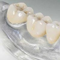 Flexible removable dentures: design, features and benefits Varieties of soft dentures with photos